During the development of electronic equipment, the stage of wiring boards design is one of the most time-consuming. In the shortest possible time, we will lay out printed circuit boards of any complexity for you. The size and shape of the boards – any. To start work on the development of a printed circuit board, a circuit diagram, a list of elements, a drawing or sketch with the desired placement of elements if necessary is required. For specific elements, to eliminate possible errors in the layout of the board, it is necessary to have a drawing or sketch of the element, a pinout, and a drawing of the seat.
The pcb manufacturer singapore design is carried out in CAD based on PCAD software. It is possible to use all existing types of housings for radio-electronic components with leads made with an arbitrary pitch in the metric or inch system including SMD components.
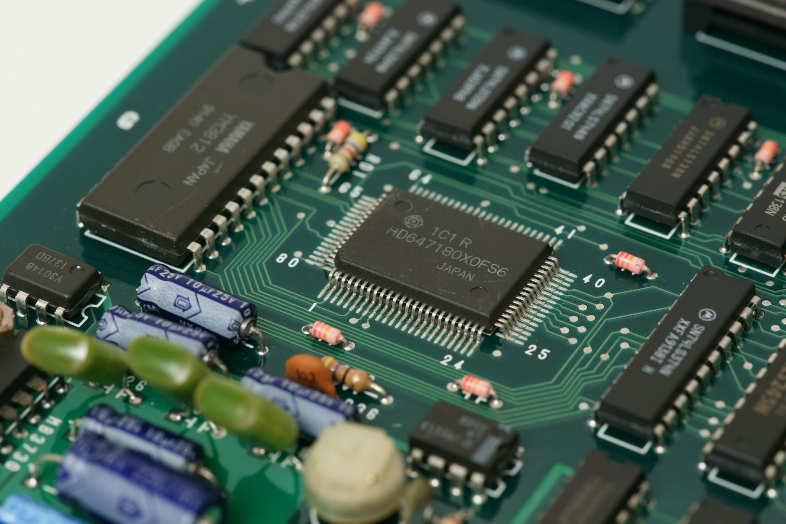
Components are placed on one or both sides of the PCB.
PCB design may include:
- Development of the topology of conductors on copper layers.
- Development of graphics of layers of a protective solder mask.
- Development of graphics for marking layers.
When laying out a board, you have to solve several tasks:
- Creating a library of missing components.
- Translation of an electrical circuit diagram from a drawing or sketch into electronic form.
- Entering the circuit board outline, mounting and fixing holes from the drawing.
- Placement of components on the printed circuit board.
- Drawing power and ground bus screen and polygons.
- Tracing wiring of the printed circuit board.
- Preparation of the board for manufacturing.
- The development of the board ends with the release of the necessary design documentation as agreed with the customer board drawing, assembly drawing, and layer drawings.